Overview
Review important deadlines, topic areas, and technical focus to prepare your submission for IEDM 2026.
Call for Papers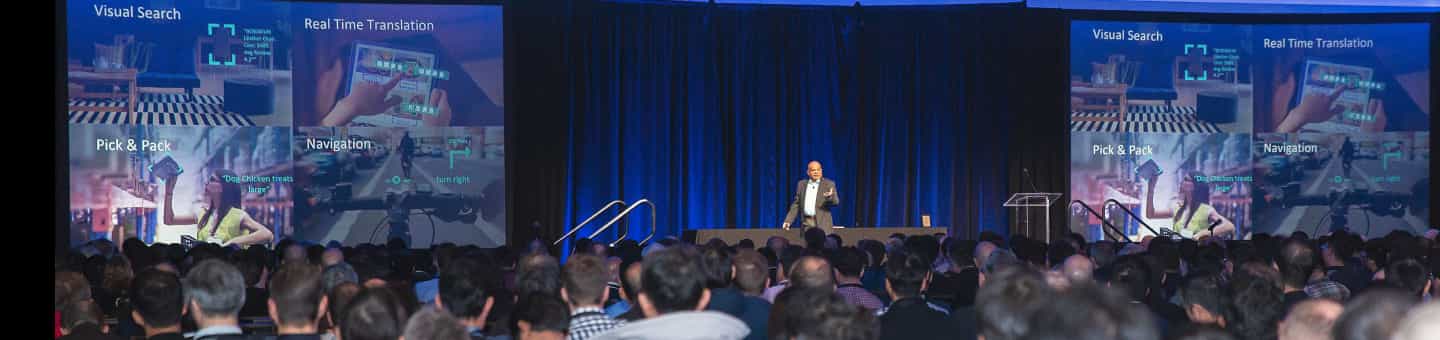
Key Dates
The IEDM 2026 Submission Site Open, submission deadline: July 16, 2026.
Late News Submission opens: August 3, 2026
Late News Deadline: August 18, 2026
The paper submission deadline will be July 16 for submission of four-page, camera-ready papers to provide faster dissemination of the conference’s cutting-edge results. Accepted papers will be published as-is in the proceedings.
General Call for Papers Topics
- Advanced Logic Technology platform and its diversified applications
- Advanced memory technologies
- Advanced packaging, 3D, chiplets, and package-device level interactions
- Advanced power devices, modules, integration, and systems
- AI, including Deep Learning and new compute paradigms
- Devices/circuits/system interaction
- Devices for RF, 5G/6G, THz and mm-wave
- Device simulation and modeling for emerging technologies
- Implantable and wearable devices
- In-memory computing
- Neuromorphic computing and AI accelerators
- Non-charge-based materials, devices and systems
- Novel materials, increased sustainability, and innovative applications for next generation devices
- Optoelectronics, displays and imaging systems
- Quantum computing and sensing devices
- Reliability and security of electronic devices, circuits, and systems
- Sensors, MEMS and bioelectronics
- Silicon Photonics
Everything Speakers Need to Prepare and Present
Papers are solicited in the areas of CMOS platform technologies and applications (e.g., HPC, LOP, mobile, automotive, low-temperature CMOS, etc.), logic devices and circuits, process integration schemes for advanced nodes, innovations in materials, process, and metrology techniques, design technology co-optimization (DTCO) and system technology co-optimization (STCO), especially to meet demands in the AI era. Platform technologies include state-of-the-art Si and beyond-Si channel devices, gate-all-around devices, stacked devices with different polarity transistors, advanced interconnect, novel power distribution integration schemes, heterogeneous 2.5D/3D integration schemes, and BEOL-compatible transistors. Device architecture, device design and analysis, process integration, module advancements in process and patterning, metrology, physical layout effects, techniques for reduced variability, yield, thermal management, methodologies, and solutions for DTCO/STCO in the solicited areas are of high interest.
Typical Themes
- CMOS platform technologies & opportunities
- Logic device performance and circuit design challenges
- Advanced, novel process integration schemes and (applications-driven) scaling approaches
- Innovations and advances in process control and metrology.
- Design technology co-optimization (DTCO), System technology co-optimization (STCO)
New or Trending Areas
- GAA (Gate-All-Around) nanosheet-based devices and circuits; novel channel materials.
- Sequential, monolithic 3D integration, heterogenous chiplets, 2.5/3D integration, thermal management
- Logic for memory
- Interconnects (BEOL, Backside power delivery)
- BEOL compatible transistors
Papers are solicited on emerging nano-electronic devices and physics. This includes devices based on novel transport and control mechanisms such as tunnel FET, negative capacitance FET, cold-source FET, cryogenic devices, topological materials and devices, phase transitions, ferroelectrics and quantum effects. Devices based on low‐dimensional systems including 2D materials, CNTs, nanowires, single electron transistors and quantum dots are welcomed. Exploratory devices with novel device functions and/or novel materials for neuromorphic compute, approximate, probabilistic and analog compute, and non-charge-based compute such as spintronics are key topics. Furthermore, emerging state machines and time dynamical compute systems are also of interest. Qubit devices as well as devices and systems designed to enable quantum computing, quantum simulation and quantum annealing are of high interest. Papers in EDT focus primarily on device physics and novel elaboration concepts.
Typical themes:
- 2D and devices on low-dimensional materials
- Novel channel materials and devices
- Non-CMOS emerging devices
- Devices for neuromorphic and approximate computing
- Spintronic and magnetic devices
- Steep-slope devices
- Quantum computing devices
New or trending areas:
- Topological materials and devices, and phase transitions transistors
- Emerging state machines, time dynamical systems, approximate computing
- Novel cryogenic devices
Papers are solicited across various domains in memory and storage technologies. This encompasses advancements and scaling in established technologies like SRAM, DRAM, and Flash, as well as breakthroughs in emerging innovations such as MRAM, PCM, FRAM, RRAM, ECM, SOM Cross-Point memory, organic memory, and NEMS-based memory. These include research pertaining to materials and devices for memory and selector in electrostatic and atomistic switching mechanisms, as well as the design and implementation of memory cells and arrays in 3D constructs, including stacking and tiering, alongside read/write access mechanisms. Additionally, submissions of novel approaches to homogenous or heterogenous integration and manufacturing techniques of memory in semiconductor fabrication or packaging assembly are welcome. Papers not mainly focused on improvements of memory FoMs but are disclosing novel computing architecture or algorithms such as CiM may be transferred to other technical sections such as EDT or NC at the discretion of the committee.
Typical Themes
- Advancements in embedded and stand-alone memories
- Emerging memories
- 3D memory technologies
- Memories (such as HBM) for AI or near memory computing applications
- In-Package Memory for PPA augmentation
New or Trending Areas
- Memories to break the memory wall
- Memory-enabled artificial intelligence applications
- Memory-Logic 3D stacking
- System-technology co-optimization
- Memory Pooling and communication
- New memory hierarchy
Papers are solicited on theoretical or computational studies of electronic devices, including logic, memory, optical components, interconnects, power related devices, display, sensors, MEMS, and bioelectronics. The approaches used in the study may include analytical, numerical, statistical, and machine-learning/AI-based methods applied to structures ranging from atomistic to device dimensions, and up to full-chip dimensions, including physics-based compact modeling. Central to submissions is the innovation of devices, whether through predictive insight into novel device concepts, predictive analysis demonstrating significant device improvements, breakthroughs in theoretical understanding of device operation, advancements in knowledge of device processing facilitating enhanced device performance, novel insights into variability, reliability, and yield issues, or breakthroughs in device optimization based on DTCO and STCO. Topics also include ab-initio/atomistic materials modeling, neuromorphic computing modeling, quantum computing and quantum-resilient hardware modeling, spintronics, low-dimensional devices, ferroelectrics, thermal modeling, optoelectronics, displays and imaging systems modeling, power devices, millimeter-wave and analog technologies, 3D/heterogeneous integration and advanced packaging modeling, electro-chemical/mechanical devices, bio-nano sensors for brain-computer interfaces and innovation in compact modeling. Encouragement is given for comparison with experimental data, model calibration, and utilization of multi-scale simulation chains.
Typical Themes
- Technology CAD and AI-driven benchmarking
- Advanced logic and memory device modeling
- Atomistic material, process, and interconnect simulation
- Compact models for DTCO and STCO
- Alternative computing device modeling including Neuromorphic and In-Memory Computing
- Optoelectronics, display and image systems modeling
- Sensors, MEMS and bioelectronics modeling
- Power, millimeter-wave, and analog technology modeling
New or Trending Areas
- Multi-scale simulation with Generative AI and hybrid techniques
- Advanced packaging, Chiplet-based, and 3D integration modeling
- Thermal modeling for high-power density and 3D stacks
- Low-temperature and quantum-resilient, and quantum device modeling
- Device modeling for photonics and optical interconnects
- Device modeling for in-memory and in-sensor computing
Papers are solicited on advancements in semiconductor memory and logic devices, as well as the circuits and algorithms that leverage them, for new and unconventional compute paradigms. Specific areas of interest span neuromorphic computing and advanced artificial intelligence (AI) acceleration techniques, broadly encompassing analog/mixed- signal computing, compute-in-memory (CIM) devices and circuits for advanced AI workloads, probabilistic computing, and bio-inspired computing such as spiking neural networks, reservoir computing, combinatorial optimization, and content-addressable memory. Use cases across the compute continuum—from the datacenter to the edge (e.g., in-sensor computing)—are highly contemplated. Submissions demonstrating novel device concepts that fundamentally improve computational efficiency, full hardware integration, explicit device-algorithm co-optimization to mitigate non-ideal device properties, and real-world applications are of highest interest. Papers focusing primarily on near-memory computing may be transferred to the MT subcommittee, while papers centered on optical or quantum computing may be transferred to EDT, at the discretion of the committee.
Typical Themes
- Memory, logic, and nanoelectronic devices featuring novel functions and/or materials, engineered for new and unconventional compute paradigms
- Analog or digital AI accelerators based on compute-in-memory (CIM) architectures driven by advanced memory technologies, including SRAM, DRAM, Flash, ReRAM, MRAM, PCRAM, ECRAM, ferroelectric memory, and memory selectors
- Probabilistic and approximate computing enabled by the stochastic behaviors of emerging devices and materials
- Emerging computing algorithms specifically enabled by memory, logic, and nanoelectronic devices
New or Trending Areas
- Hardware acceleration for generative AI and LLMs
- On-chip learning and edge intelligence enabled by novel device dynamics
- Neuromorphic sensors and in-sensor computing
- Monolithic 3D and heterogeneous integration for scalable computing
- Device-algorithm co-optimization
Papers are solicited on optoelectronics, displays, and imaging systems. This includes novel devices, structures, and integration for image sensors, displays, light sources, photonic devices, and high-speed photodetectors and modulators. New technologies on heterogeneous integration of optoelectronics devices as well as on photonic-electronic integration for optical interconnects, on-chip networks and sensing are welcomed. Papers on quantum photonics, neuromorphic photonics, and plasmonics for quantum computation, sensing and encryption are also of interest. Furthermore, ODI includes CMOS imagers, high-speed and high-time resolution imagers, tacked imagers sensors, single-photon sensitivity, Time-Of-Flight and non-visible image sensors. In addition, papers on displays of all types, for augmented or virtual reality, holography, TFTs for photonics applications, flexible, stretchable, and/or printed electronics, in-display sensors are encouraged. Papers on displays or light emitting devices with novel materials such as perovskites or quantum dots are also of interest.
Typical Themes
- Heterogeneous optoelectronic integration including sources, modulators, or detectors
- Neuromorphic photonics technologies
- Single photon emitters and detectors
- Luminescent devices based on new materials including perovskites and quantum dots
- Displays and imagers for augmented or virtual reality
- Holographic devices and displays
- Displays with unconventional form or size
- Photodetectors and imagers with new materials or flexible platform and printed electronics
- Imagers with ultra-miniaturized pixels, spectral bandwidth beyond visible, high sensitivity, or high time-resolution,
- Image sensors with pixels for range sensing, TOF, RGBZ, LIDAR
New or Trending Areas
- Silicon photonics
- Photonic devices for quantum computation and sensing
- Intelligent Image Sensors, Advanced On-chip optics for imagers
- In-display and under-display Sensors
Contributions are sought on novel circuit topologies, manufacturing processes, supporting modeling (TCAD and compact models), device physics, reliability, and materials (Si, III-Vs, SiC, (Al)GaN, Ga2O3, AlScN, LiNbO3, diamond, LTO, BN, etc.) along with fundamental studies on doping, deep-level traps, interface states, and device reliability for power switching and high frequency devices. Papers are solicited on discrete and integrated power and high frequency (micro, mm-wave and THz) devices and physics, modules and systems. Topics of interest include devices (diodes, BJTs, FETs, super-junction devices, heterostructures, IGBTs, HEMTs, HBTs, light- triggered structures for galvanic isolation and faster switching, bi-directional switches, vertical geometry devices, RF acoustic resonators, SAW and BAW filters, etc.) and device/package/circuit interactions, including thermal management. A wide variety of applications are also within the scope of PMA: (power conversion, supply, regulation and conditioning for computers and data centers, motor drives, transportation, solar, wind, smart grid applications, wireless power harvesting/transfer, filters, beam formers, power amplifiers, tunable passives, antenna arrays).
Typical Themes
- Power and high speed (microwave to THz devices) devices, modules, and systems
- Manufacturing processes, device design, modeling, physics, and reliability of power and high-speed devices
- Fundamental studies on doping, traps, interface states, and device reliability for power and high-speed switching devices
- Micro and mm-wave devices, such as power amplifiers, low noise amplifiers, switches and mixers.
- Energy harvesting devices and circuits
New or Trending Areas
- Wide bandgap and ultra-wide bandgap semiconductors such as SiC, (Al)GaN, diamond, β-Ga2O3, BN
- Emerging ferroelectric materials and devices: Al(Sc)N, Al(Y)N, …
- Power devices for applications from automotive and aviation to smart grid
- Devices and circuits for 5G and 6G
- Extreme environment power and high-speed devices
Papers are solicited that focus on component-level FEOL/MOL/BEOL characterization and reliability modeling, reliability evaluation, both experimental and modeling, of devices dedicated to analog, logic, and memory applications, interconnects, circuits, and systems. In addition to Si-based technologies, authors are encouraged to submit their recent achievements made employing other material systems, such as SiGe, IGZO, ferroelectric materials, 2D materials, etc. The reliability topics include, for FEOL, transistor degradation due to hot carriers, bias temperature instabilities, random telegraph noise, dielectric SILC and breakdown as well as modeling the aging and wearout behavior. For MOL/BEOL, topics include the breakdown of MOL spacers and BEOL dielectrics, electromigration, and stress migration failures of contacts and interconnects. For product, system, and circuit reliability, topics include latch-up, ESD, soft error mechanisms, variability-aware design, and design for reliability, robustness, and security of electronic circuits and systems. Of particular interest are investigations of degradation mechanisms for devices, circuits, and systems in the following areas: conventional and emerging memories; beyond CMOS devices; 3D IC package reliability; more-than-Moore applications; biomedical devices and systems; automotive and aerospace.
Typical Themes
- Component-level FEOL/MOL/BEOL characterization and reliability modeling
- Reliability of conventional and emerging memories
- Circuits, systems-level reliability, and aging
- Thermal and PID/charging management in existing and novel process integration
- Reliability of RF/mm-wave/5G in high-frequency applications
- Reliability of devices, circuits, and systems for more-than-Moore applications,
- automotive, aerospace and bio-applications (BioFETs, DNA detection, etc.)
- Reliability of cryogenic devices for future quantum computing applications
New or Trending Areas
- Reliability of new materials and/or new architectures for transistors
- Reliability of advanced 2.5D/3D IC advanced package
- Design for testing (DFT) / Design for reliability (DFR) solutions for improved reliability
- Robustness and security of electronic circuits and systems
Papers are solicited in the areas of sensors, MEMS/NEMS, microfluidics and lab-on-chip, BioMEMS, and bioelectronic devices and systems, with emphasis on new device concepts, integrated CMOS implementations, embedded intelligence, and multifunctional microsystems for applications in health, communication, mobility, energy, defense, and extreme environments. Sensors include chemical, biological, acoustic, electrical, electrochemical, magnetic, and mechanical modalities. Topics of interest include physical and biochemical sensors, actuators, resonators, inertial microsystems, RF MEMS, SAW/BAW and acoustic devices, optomechanical devices, energy-harvesting and micro- power devices, and microsystems that integrate sensing, actuation, readout, control, and packaging. Bioelectronics covers hybrid organic/inorganic devices, point-of-care and implantable systems, neural and bioelectronic interfaces, flexible and soft devices, multimodal biomedical sensing, and nanosensors for brain-computer interfaces.
Typical Themes
- Physical, chemical, biological, and multimodal integrated sensors
- MEMS/NEMS resonators, oscillators, actuators, and inertial microsystems
- RF MEMS, SAW/BAW, acoustic, and optomechanical devices
- Energy harvesting, micro-power generation, and on-chip storage
- Microfluidic, lab-on-chip, BioMEMS, and biomedical microsystems
- Bioelectronic, implantable, flexible, and soft devices and interfaces
New or Trending Areas
- Intelligent sensors and microsystems with embedded AI
- In-sensor computing and in-MEMS computing
- Wave-based and non-charge-based computing paradigms
- Phononic, acoustic, and magnetoacoustic devices for RF, sensing, and information processing
- Extreme-environment microsystems, including sensing, readout, control, and packaging
- Multifunctional microsystems integrating sensing, actuation, computation, and communication on chip