
Explore Expert Keynote
Kick-off IEDM on Monday morning with 3 keynote presentations from leaders in the industry.
Registration
Keynote Session | Monday, December 14
Session 1.1 | AI Driven Semiconductor Paradigm Shift: Optimizing the Semiconductor Industry from Device Scaling to System Integration
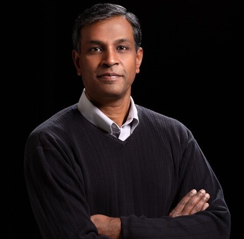
Session 1.2 | Driving AI Memory Innovation: From Device Technology to AI Memory Platform

Session 1.3 | Technology Trends in the IDM Semiconductor Business

Artificial intelligence is no longer a distant idea or a science-fiction concept. It is here, and it is already transforming how we live, work, discover, and innovate. Large language models have expanded the realm of what is possible in ways that seemed unimaginable only a few years ago. Yet behind every AI breakthrough is a critical foundation: semiconductor technology. Semiconductors are enabling the AI revolution, and AI is now reshaping the future of semiconductors. It is driving the need for higher-performance, more energy-efficient compute while challenging the traditional limits of CPU scaling and system architecture. As AI moves from massive cloud-training environments to real-time inference at the edge, the requirements are becoming extraordinary: more memory, more bandwidth, lower latency, and far greater efficiency. Meeting this moment will require more than incremental improvement. We must innovate across the full stack—from materials and devices to architectures, packaging, and manufacturing—to deliver the performance per watt, memory bandwidth, and reliability the AI era demands.
This is why technology roadmaps are moving faster than ever before. Across the full stack, we are seeing a powerful new wave of innovation. Transistor architecture is evolving from FinFETs to gate-all-around structures, enabled by new channel materials, new interconnect metals, and new power-delivery schemes. Power delivery is also moving from the front side to the back side of the wafer, opening new design space and creating new opportunities for performance and efficiency. Looking ahead, Complementary Field Effect Transistor (CFET) technology—combined with backside innovation—has the potential to reshape the industry again by enabling more compact layouts, higher computational throughput, and improved power efficiency. At the same time, heterogeneous integration is accelerating rapidly. EMIB, hybrid bonding, and chiplets are no longer future concepts; they are becoming essential building blocks for AI systems.
The reason is clear: AI is a data-movement challenge as much as it is a compute challenge. Domain-specific accelerators, increasingly specialized CPUs, and tightly coupled memory hierarchies are essential to remove bottlenecks and keep data flowing efficiently. Memory–compute integration—including high-bandwidth memory, near-memory processing, in-memory compute, and advanced 2.5D and 3D stacking—offers a powerful path to reduce energy-intensive data movement and sustain performance growth beyond the limits of monolithic scaling. Emerging technologies such as silicon photonics and optical interconnects can help overcome the limitations of electrical interconnects while significantly improving energy efficiency. And with Embedded Multi-Die Interconnect Bridge-TSV (EMIB-T), we can enable faster, more power-efficient, and more customizable connectivity between AI accelerators and high-bandwidth memory.
But as we transform the technology, we must also transform how we qualify it. Traditional device-centric qualification will not be sufficient for the systems we are building. The future requires system-level qualification that accounts for heterogeneous dies, advanced interconnects, thermal gradients, power-delivery integrity, data retention, and workload-dependent degradation. Quality must move earlier in the lifecycle, supported by stronger defect detection, richer traceability from materials to package, predictive reliability models, and tighter feedback loops across design, process control, test, and field operation. Just as importantly, we must embed sustainability and ethics into the foundation of our work. The AI-intensive future will carry environmental and social costs unless we act now. That means moving beyond carbon offsets toward intrinsic sustainability—designing systems that are efficient by nature—and advancing an equitable intelligence model supported by greater supply-chain transparency.
This is the opportunity before us. AI demand and semiconductor scaling are converging to redefine manufacturing as an integrated, reliability-led platform for the next generation of compute. The demands of AI hardware will continue to grow, and the choices we make today will determine how responsibly and sustainably that growth is realized. We have both the opportunity and the responsibility to shape this future with purpose, discipline, and bold innovation.
Speaker Bio
Naga Chandrasekaran is executive vice president, chief technology and operations officer, and general manager of the Intel Foundry organization at Intel Corporation. He is responsible for Intel Foundry’s technology development, worldwide manufacturing, customer service and ecosystem operations, including research, development, and deployment of next-generation silicon logic, packaging and test technologies, as well as front-end and back-end manufacturing, foundry services, strategic planning, corporate quality and reliability and supply chain.
The Intel Foundry business brings together all the critical components that fabless customers need to design and manufacture chips for the new era of AI-driven computing.
Previously, Chandrasekaran was general manager of Foundry Technology and Manufacturing, overseeing Intel Foundry’s technology development and global manufacturing operations. Prior to joining Intel, Chandrasekaran served in senior leadership roles at Micron, most recently as senior vice president of Technology Development. He led Micron’s global technology development and engineering efforts related to the scaling of current memory technologies, advanced packaging technology and emerging technology solutions. Before that, he served as Micron’s senior vice president of Process R&D and Operations.
Chandrasekaran earned a bachelor’s degree in mechanical engineering from the University of Madras; a master’s degree and a doctorate in mechanical engineering from Oklahoma State University; a master’s degree in information and data science from the University of California, Berkeley; and dual executive MBAs from the University of California, Los Angeles, and the National University of Singapore.
As AI workloads continue to scale, overall system performance is increasingly determined by the interplay between compute and memory performance. This drives demand for high bandwidth, power efficiency, and reliability. Limits in Cell scaling has accelerated the transition from 2D to 3D memory architectures and, as this shift progresses, the competitive performance of AI memory products is now increasingly driven by Peripheral (Peri) transistor technology.
Wafer bonding technology is fundamentally reshaping memory architecture by decoupling Cell and Peripheral wafer fabrication. This separation enables the integration of various performance boosters and allows for the independent optimization of Peripheral (Peri) technology. However, this shift alone does not guarantee successful innovation in the memory domain. Memory systems remain stringently constrained by cost reduction, the need for high-voltage operation, pitch-limited design rules, leakage control, and reliability requirements. Furthermore, the increasing complexity of HBM and future 3D architectures introduces additional challenges, such as thermal management. Consequently, the industry is shifting from simply adapting logic technologies to developing memory-specific solutions, including dedicated HKMG, RMG, and FinFET architectures tailored for the unique constraints of memory environments.
Furthermore, advances in memory-optimized design methodologies are imperative. Because memory technology and design are developed concurrently, accurate pre-layout modeling is essential for rapid design exploration. Memory design also continues to evolve from full-custom toward hybrid custom-digital methodologies. Building on this foundation, AI-native DTCO and STCO frameworks extend optimization across device, circuit, package, and system levels.
The convergence of Peri device innovation and memory-native design methodologies establishes a new AI Memory Platform paradigm. This paradigm enables workload-specific memory solutions built upon a common technology foundation, thereby transforming memory from a commodity into a strategic enabler of AI systems.
Speaker Bio
Yunik Son is Vice President of Device Technology Solution (DTS) at SK hynix, where she leads device technology development for DRAM and NAND memory products. She has contributed to the development of advanced transistor technologies and played a key role in the development and adoption of High-K Metal Gate (HKMG) technology for memory products. Her research interests include transistor technology, device modeling, reliability engineering, DTCO/STCO, AI-driven semiconductor development, and advanced memory architecture. She received the Korean Engineer Award for her contributions to memory
technology innovation.
In recent years, two game changers have been reshaping IDM processes i.e. fab digitalization and advanced packaging. Digitalization links front-end modeling, device and circuit simulation, manufacturing analytics, and system-level validation into a continuous flow, accelerating learning and optimization. In parallel, advanced packaging, including panel-level packaging and wafer-to-wafer hybrid bonding, enables heterogeneous integration of logic, memory, power, sensors, and connectivity, allowing each application to combine the most suitable technologies for higher system performance. Building on these enablers, ST is pursuing three complementary technology trends.
- Silicon photonics provides fast, energy-efficient communication for AI server infrastructure.
- Expanding computing from advanced microcontrollers and edge AI to quantum computing.
- Sensing and actuation, based on imaging, MEMS, and power technologies, connect the physical and digital worlds for smarter automotive, industrial and personal electronics applications.
Full automation and robotics in manufacturing complements the new way of R&D in a fully virtual environment exploiting ST’s diversified technology portfolio. The IDM structure enables design-technology co-optimization and greater system-level flexibility.
Speaker Bio
Fabio Gualandris is STMicroelectronics’ President, Quality, Manufacturing, and Technology and has held this position since July 2023. He was responsible for the company’s Back-End Manufacturing & Technology organization since 2016 and also led the Company’s Testing Council, alongside its manufacturing strategy in Asia and efforts in System-in-Package technology. Gualandris is a member of ST’s Executive Committee.
Gualandris joined SGS Microelettronica (now ST) R&D in 1984. He became R&D Director of Operations in 1989 and became Automotive BU Director in 1996. After two years as President and CEO of Semitool, he rejoined ST in 2000 as Group VP responsible for memory products including the RAM/PSRAM and Automotive Flash. In 2005, Gualandris was appointed CEO of ST Incard, an ST smart-card subsidiary. In 2008-2010, he served as VP and Supply Chain General Manager at ST’s memory JV with Intel. In 2011, Gualandris was appointed ST’s Executive Vice President, Product Quality Excellence.
Gualandris has authored several technical and managerial papers and holds multiple international patents. He serves as Chairman of STS, ST’s manufacturing JV in China.
Fabio Gualandris was born in Bergamo, Italy, in 1959. He holds a Master’s degree in Physics from the University of Milan.